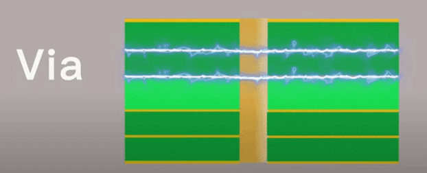
PCBWay Via Plating Thickness: The Key to Quality PCB Manufacturing! via-in-pad in pcb design manufacturing
If you are searching about PCB Via Plating: Depth Guide And Process - Jhdpcb you've visit to the right place. We have 25 Images about PCB Via Plating: Depth Guide And Process - Jhdpcb like Detailed Procedures of Plating Copper for PCB Processing - PCB, Detailed Procedures of Plating Copper for PCB Processing - PCB and also Inspirasi Pcbway Via Plating Thickness, Skema Pcb. Here you go:
PCB Via Plating: Depth Guide And Process - Jhdpcb
 jhdpcb.com
PCB Via Plating: Depth Guide And Process - Jhdpcb
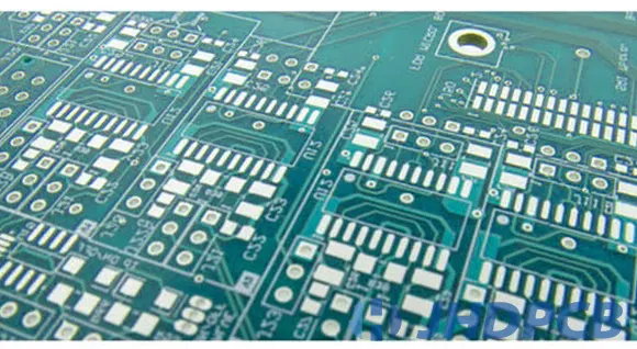
Detailed Procedures Of Plating Copper For PCB Processing - PCB
 www.pcbway.com
Detailed Procedures of Plating Copper for PCB Processing - PCB ...
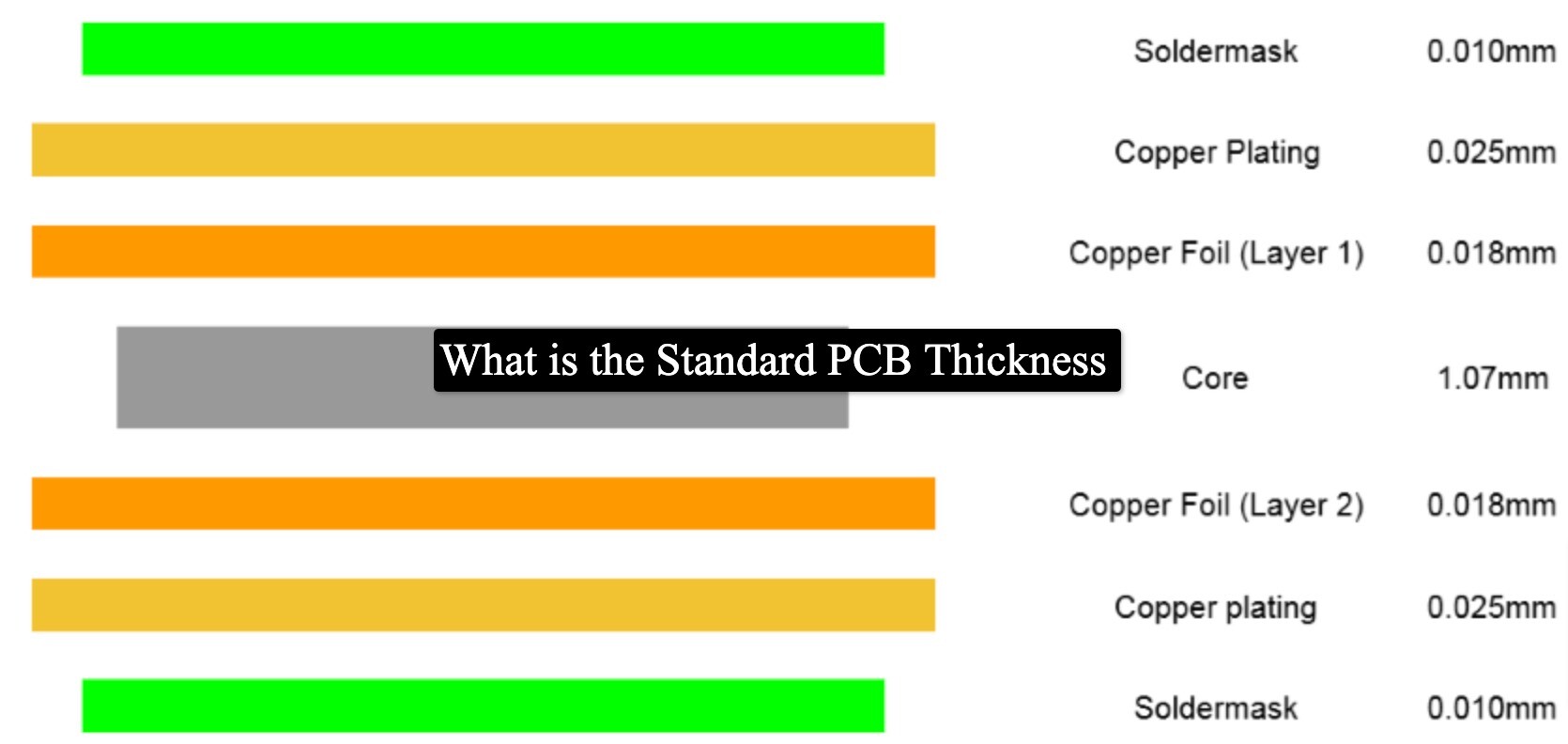
Standard PCB Thickness - Everything You Need To Know About
 absolutepcbassembly.com
Standard PCB Thickness - Everything you need to know about
The Ultimate Guide To Understanding Via Plating Thickness In PCBs - Top
 camtechpcb.com
The Ultimate Guide to Understanding Via Plating Thickness in PCBs - Top ...
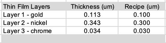
Plating Thickness Measurements - SEM Lab Inc.
 www.semlab.com
Plating Thickness Measurements - SEM Lab Inc.
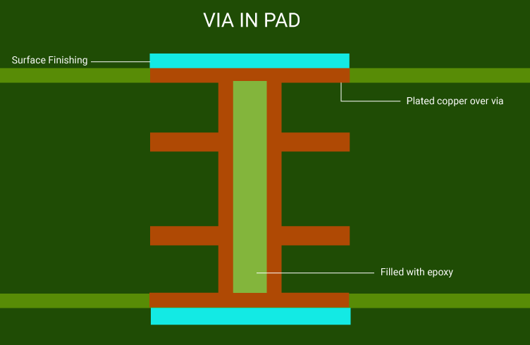
Via-in-Pad In PCB Design Manufacturing | Sierra Circuits
 www.protoexpress.com
Via-in-Pad in PCB Design Manufacturing | Sierra Circuits
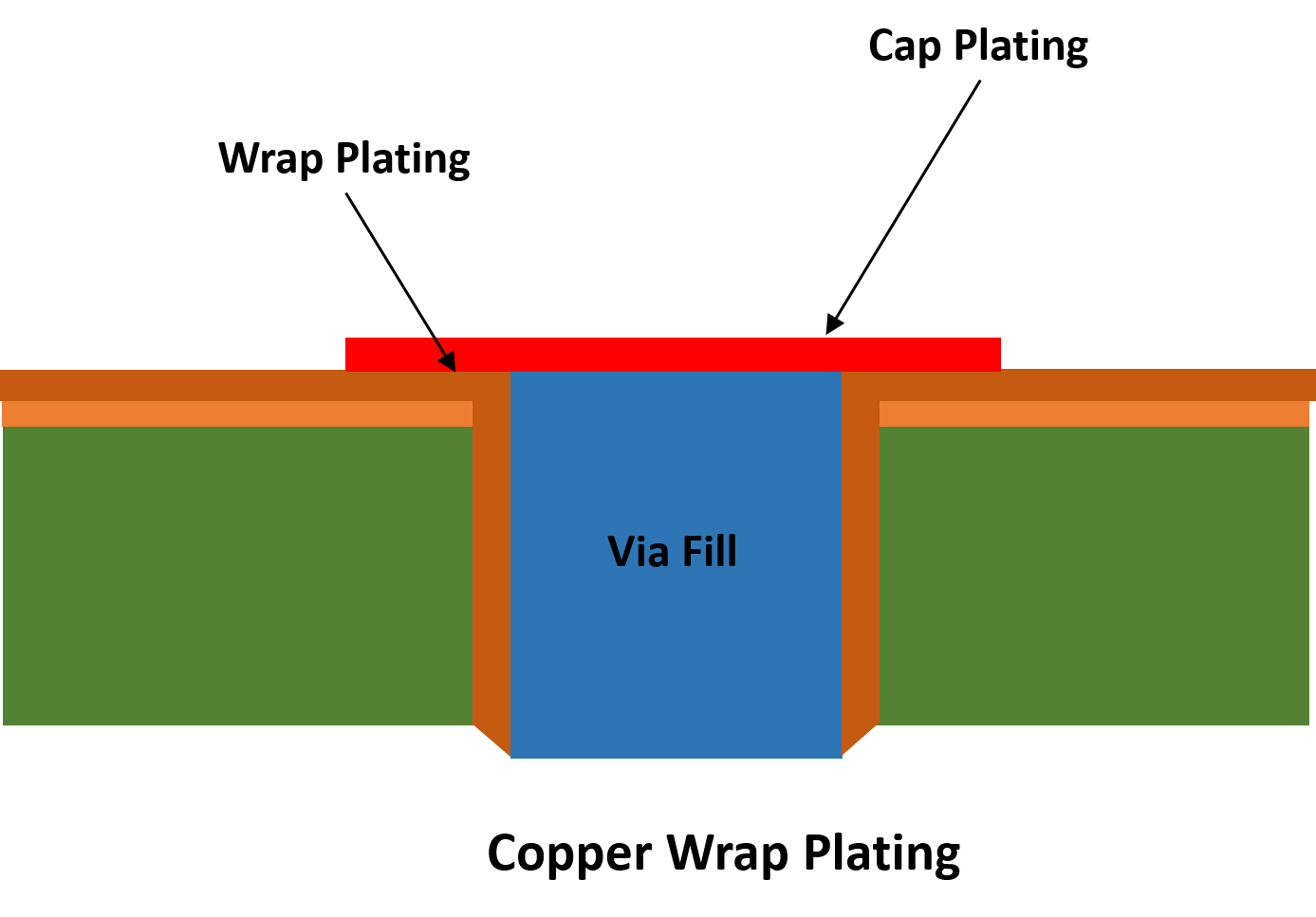
Copper Wrap Plating For PCB Manufacturing | Sierra Circuits
 www.protoexpress.com
Copper Wrap Plating for PCB Manufacturing | Sierra Circuits
The Ultimate Guide To Understanding Via Plating Thickness In PCBs - Top
 camtechpcb.com
The Ultimate Guide to Understanding Via Plating Thickness in PCBs - Top ...
Explore Excellence With Leading Gold Fingers PCB Manufacturer Services
 sfxpcb.com
Explore Excellence with Leading Gold Fingers PCB Manufacturer Services
Pcb Design - PCB Base Copper Weight Vs Plating Thickness - Electrical
 electronics.stackexchange.com
pcb design - PCB base copper weight vs plating thickness - Electrical ...
Inspirasi Pcbway Via Plating Thickness Skema Pcb - Vrogue.co
 www.vrogue.co
Inspirasi Pcbway Via Plating Thickness Skema Pcb - vrogue.co
The Ultimate Guide To Understanding Via Plating Thickness In PCBs - Top
 camtechpcb.com
The Ultimate Guide to Understanding Via Plating Thickness in PCBs - Top ...
Explaining Via-filling Plating In PCB Manufacturing Process - RayPCB
 www.raypcb.com
Explaining Via-filling Plating in PCB Manufacturing Process - RayPCB
Detailed Procedures Of Plating Copper For PCB Processing - PCB
 www.pcbway.com
Detailed Procedures of Plating Copper for PCB Processing - PCB ...
PCB & PCB Assembly Reviews - Share - PCBWay
 www.pcbway.com
PCB & PCB Assembly Reviews - share - PCBWay
Why Some PCBs Need Edge Plating? - Technology - PCBway
 www.pcbway.com
Why Some PCBs Need Edge Plating? - Technology - PCBway
Inspirasi Pcbway Via Plating Thickness, Skema Pcb
 skemadriver.blogspot.com
Inspirasi Pcbway Via Plating Thickness, Skema Pcb
The Ultimate Guide To Understanding Via Plating Thickness In PCBs - Top
 camtechpcb.com
The Ultimate Guide to Understanding Via Plating Thickness in PCBs - Top ...
The Ultimate Guide To Understanding Via Plating Thickness In PCBs - Top
 camtechpcb.com
The Ultimate Guide to Understanding Via Plating Thickness in PCBs - Top ...
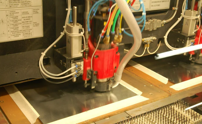
PCB Manufacturing Process & Equipment - PCBWay
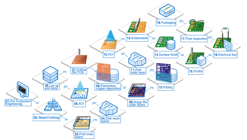 www.pcbway.com
PCB manufacturing Process & Equipment - PCBWay
Inspirasi Pcbway Via Plating Thickness, Skema Pcb
 skemadriver.blogspot.com
Inspirasi Pcbway Via Plating Thickness, Skema Pcb
The Ultimate Guide To Understanding Via Plating Thickness In PCBs - Top
 camtechpcb.com
The Ultimate Guide to Understanding Via Plating Thickness in PCBs - Top ...
The Ultimate Guide To Understanding Via Plating Thickness In PCBs - Top
 camtechpcb.com
The Ultimate Guide to Understanding Via Plating Thickness in PCBs - Top ...
Inspirasi Pcbway Via Plating Thickness, Skema Pcb
 skemadriver.blogspot.com
Inspirasi Pcbway Via Plating Thickness, Skema Pcb
Inspirasi Pcbway Via Plating Thickness, Skema Pcb
 skemadriver.blogspot.com
Inspirasi Pcbway Via Plating Thickness, Skema Pcb
The ultimate guide to understanding via plating thickness in pcbs. Explore excellence with leading gold fingers pcb manufacturer services. The ultimate guide to understanding via plating thickness in pcbs